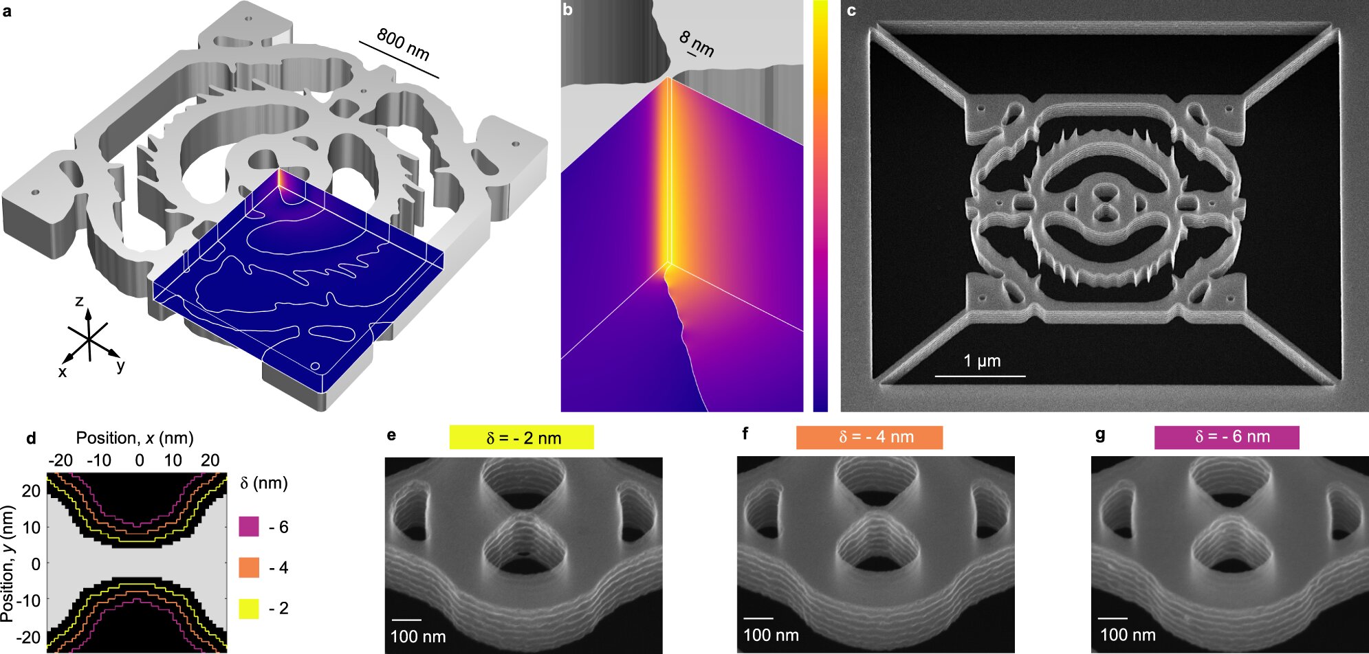
. a Rendering of the DBC design generated by tolerance-constrained topology optimization. The normalized ∣E∣-field is projected on the faces defining the three symmetry planes of the design. b Zoom-in of the solid silicon bowtie exhibiting a strong field confinement due to the bowtie bridge dimension of 8 nm. c 40° tilted scanning electron microscopy (SEM) image of a fabricated cavity. d Global geometry-tuning, δ. Each air (black) pixel (1 nm<sup>2</sup>) inside a contour δ is uniformly exposed by electron beam lithography; therefore, the air characteristics defining the device are set uniformly. for example, 40° tilted SEM images of the bowtie region for δ = {−2, −4, −6} nm. We measure the average width of fabricated bow ties at (8 ± 5) nm, (10 ± 5) nm, and (16 ± 5) nm for Figures e, f, and g, respectively, noting the variation in width along the z-direction caused by the scallops and negative flank angle of about 1° represented by the uncertainty, as shown in the main text. Credit: <i>Nature Communication</i> (2022). DOI: 10.1038/s41467-022-33874-w” width=”800″ height=”383″/><figcaption class=") Fabrication of a Topology Optimized Dielectric Silicon Bowtie Cavity (DBC). a Rendering of the DBC design generated by optimizing the constrained-to-tolerance topology. The normalized ∣E∣ field is projected on the faces defining the three planes of symmetry of the drawing. b Zoom in of the solid silicon bow tie showing strong field confinement due to the butterfly bridge dimension of 8 nm. c Scanning electron microscopy (SEM) image tilted at 40° of a fabricated cavity. d Global geometry setting, δ. Each air pixel (black) (1 nm2) inside a contour δ is uniformly exposed by electron beam lithography; therefore, the air characteristics defining the device are set uniformly. for example, 40° tilted SEM images of the bowtie region for δ = {−2, −4, −6} nm. We measure the average width of fabricated bow ties at (8 ± 5) nm, (10 ± 5) nm, and (16 ± 5) nm for Figures e, f, and g, respectively, noting the variation in width along the z-direction caused by the scallops and negative flank angle of about 1° represented by the uncertainty, as shown in the main text. Credit: Nature Communication (2022). DOI: 10.1038/s41467-022-33874-w
Fabrication of a Topology Optimized Dielectric Silicon Bowtie Cavity (DBC). a Rendering of the DBC design generated by optimizing the constrained-to-tolerance topology. The normalized ∣E∣ field is projected on the faces defining the three planes of symmetry of the drawing. b Zoom in of the solid silicon bow tie showing strong field confinement due to the butterfly bridge dimension of 8 nm. c Scanning electron microscopy (SEM) image tilted at 40° of a fabricated cavity. d Global geometry setting, δ. Each air pixel (black) (1 nm2) inside a contour δ is uniformly exposed by electron beam lithography; therefore, the air characteristics defining the device are set uniformly. for example, 40° tilted SEM images of the bowtie region for δ = {−2, −4, −6} nm. We measure the average width of fabricated bow ties at (8 ± 5) nm, (10 ± 5) nm, and (16 ± 5) nm for Figures e, f, and g, respectively, noting the variation in width along the z-direction caused by the scallops and negative flank angle of about 1° represented by the uncertainty, as shown in the main text. Credit: Nature Communication (2022). DOI: 10.1038/s41467-022-33874-wUntil recently, it was widely believed among physicists that it was impossible to compress light below the so-called diffraction limit (see below), except by using metallic nanoparticles, which unfortunately also absorb light. It therefore seemed impossible to strongly compress light in dielectric materials like silicon, which are key materials in information technology and have the important advantage of not absorbing light.
Interestingly, it was theoretically demonstrated in 2006 that the diffraction limit does not apply to dielectrics either. Yet no one has managed to show it in the real world, simply because no one has been able to build the necessary dielectric nanostructures until now.
A DTU research team has successfully designed and built a structure, called a dielectric nanocavity, which concentrates light into a volume 12 times lower than the diffraction limit. The result is revolutionary in optical research and has just been published in Nature Communication.
“Although computer calculations show that you can focus light to an infinitesimally small point, this only applies in theory. Actual results are limited by how small details can be achieved, for example, on a chip,” says Marcus Albrechtsen, Ph.D.-student at DTU Electro and first author of the new paper.
“We programmed our knowledge of actual photonic nanotechnology and its current limitations into a computer. Then we had the computer find a pattern that collects photons in an unprecedented area – in an optical nanocavity – that we were also able to build in the lab.”
Optical nanocavities are structures specially designed to trap light so that it does not spread as we are used to but projects it back and forth as if you put two mirrors face to face. The closer you bring the mirrors together, the more intense the light between the mirrors becomes. For this experiment, the researchers designed a so-called bowtie structure, which is particularly effective at squeezing photons together due to its particular shape.
The nanocavity is made of silicon, the dielectric material on which the most advanced modern technology is based. The material for the nanocavity was developed in DTU’s cleanroom laboratories, and the models on which the cavity is based are optimized and designed using a unique topology optimization method developed at DTU. Initially developed to design aircraft bridges and wings, it is now also used for nanophotonic structures.
“It took a great joint effort to achieve this breakthrough. This was only possible because we managed to combine world-leading research from several research groups at DTU,” says Associate Professor Søren Stobbe, who led the research work.
Important breakthrough for energy efficient technology
This discovery could be decisive for the development of new revolutionary technologies that can reduce the amount of energy-consuming components in data centers, computers, telephones, etc.
The power consumption of computers and data centers continues to grow, and there is a need for more durable chip architectures that consume less power. This can be achieved by replacing electrical circuits with optical components. The researchers’ vision is to use the same division of labor between light and electrons used for the Internet, where light is used for communication and electronics for data processing. The only difference is that the two functionalities must be integrated into the same chip, which requires the light to be compressed to the same size as the electronic components. DTU’s breakthrough shows that it is, in fact, possible.
“There is no doubt that this is an important step in the development of more energy-efficient technology for, for example, nanolasers for optical connections in data centers and future computers, but there is still a long way to go,” says Marcus Albrechtsen.
The researchers will now work harder and refine the methods and materials to find the optimal solution.
“Now that we have the theory and the method in place, we will be able to manufacture more and more intense photons as the surrounding technology develops. I am convinced that this is only the first of a long series of major developments in physics and photonic nanotechnology centered on these principles,” says Søren Stobbe.
The diffraction limit
Diffraction limit theory describes that light cannot be focused to a volume less than half the wavelength in an optical system – for example, this applies to the resolution of microscopes.
However, nanostructures can consist of elements much smaller than the wavelength, which means that the diffraction limit is no longer a fundamental limit. Bowtie structures, in particular, can compress light into very small volumes limited by the size of the bowtie and, therefore, the quality of the nanofabrication.
When light is compressed, it becomes more intense, enhancing interactions between light and materials such as atoms, molecules, and 2D materials.
Dielectric materials
Dielectric materials are electrically insulating. Glass, rubber, and plastic are examples of dielectric materials, and they contrast with metals, which are electrically conductive.
An example of a dielectric material is silicon, which is often used in electronics but also in photonics.
Finding high-Q resonant modes in a dielectric nanocavity
Marcus Albrechtsen et al, Confinement of nanoscale photons in dielectric cavities with optimized topology, Nature Communication (2022). DOI: 10.1038/s41467-022-33874-w
Provided by the Technical University of Denmark
Quote: Researchers compress light 12 times below the diffraction limit in a dielectric material (2022, October 26) Retrieved October 26, 2022 from https://phys.org/news/2022-10-compress-diffraction-limit -dielectric-material.html
This document is subject to copyright. Except for fair use for purposes of private study or research, no part may be reproduced without written permission. The content is provided for information only.
#Researchers #compress #light #times #diffraction #limit #dielectric #material